


Time:2025-09-12 Views:1 source:News
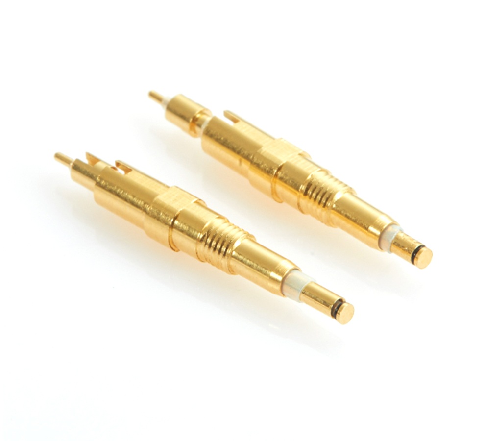
The Pogo Pin PCB distributed structure represents a specialized design approach aimed at optimizing the performance, reliability, and functionality of printed circuit boards (PCBs) integrated with Pogo Pins. In modern electronic systems, where high - speed signal transmission, power distribution, and compact designs are essential, the distributed structure of Pogo Pins on PCBs plays a crucial role.
In a Pogo Pin PCB distributed structure, the Pogo Pins are strategically placed across the PCB rather than being concentrated in a single area. This distribution serves multiple purposes. Firstly, it helps in achieving better electrical connectivity and signal integrity. By spreading out the Pogo Pins, the electrical load is more evenly distributed, reducing the risk of overheating and signal interference. For example, in high - frequency applications, having Pogo Pins distributed throughout the PCB can minimize the length of signal traces, thereby reducing signal delay and attenuation. This is particularly important in systems where precise and rapid data transfer is required, such as in high - performance computing and telecommunications equipment.
Secondly, the distributed structure enhances mechanical stability. Pogo Pins are often used to establish electrical connections between different components or modules. When these pins are distributed, they provide a more balanced support system, reducing the stress on the PCB and the connected components. This is especially beneficial in applications where the PCB may be subject to vibrations, shocks, or mechanical stresses, such as in automotive electronics or aerospace systems. A well - designed distributed Pogo Pin structure can prevent mechanical failures and ensure the long - term durability of the PCB assembly.
The design of a Pogo Pin PCB distributed structure involves careful consideration of several factors. The layout of the Pogo Pins needs to be optimized based on the electrical requirements of the system, including the type of signals (e.g., digital, analog), power levels, and the overall circuit topology. Additionally, the physical dimensions of the Pogo Pins, such as their length, diameter, and pitch, must be taken into account to ensure proper fit and functionality on the PCB. Designers also need to consider the routing of traces between the Pogo Pins and other components on the PCB. Efficient trace routing can minimize electromagnetic interference (EMI) and improve the overall performance of the system.
Manufacturing a PCB with a distributed Pogo Pin structure also presents its own set of challenges. Precise placement of the Pogo Pins during the assembly process is crucial to ensure accurate electrical connections. Advanced manufacturing techniques, such as automated pick - and - place machines, are often employed to achieve the required level of precision. Moreover, the soldering process needs to be carefully controlled to ensure strong and reliable solder joints between the Pogo Pins and the PCB pads. Quality control measures, including electrical testing and visual inspection, are essential to verify the integrity of the distributed Pogo Pin structure and the overall functionality of the PCB. In summary, the Pogo Pin PCB distributed structure is a key design element that can significantly enhance the performance and reliability of electronic systems, but it requires careful design, manufacturing, and quality control to be successfully implemented.
Read recommendations:
Magnetic PogoPin manufacturer price


159-2067-7287 Mr. Wan

0769-86006029

No. 5, Zhenrong Road, Wusha, Chang'an Town, Dongguan City
 Whatapp
CopyRight © 2024 Dongguan Yongtan New Energy Co., Ltd. All Rights Reserved


 CN
CN
 Home >