


The development of Pogo Pin array high - density packaging represents a significant advancement in the field of electrical interconnections, addressing the growing demand for smaller, more compact, and highly functional electronic devices. High - density packaging of Pogo Pin arrays allows for a greater number of electrical connections to be packed into a limited space, enabling the miniaturization of electronic products while maintaining high - performance and reliability.
In high - density Pogo Pin array packaging, the key challenge lies in the precise design and arrangement of the pins. The pins need to be positioned closely together without sacrificing the electrical and mechanical performance. Advanced design tools, such as computer - aided design (CAD) software, are used to optimize the layout of the Pogo Pin array. The design process takes into account factors such as the pitch (distance between adjacent pins), the size of the pins, and the overall dimensions of the package. A smaller pitch allows for a higher density of pins, but it also increases the difficulty of manufacturing and assembly. Therefore, a balance needs to be struck between achieving high density and ensuring manufacturability.
The manufacturing process of high - density Pogo Pin arrays is highly complex and requires advanced techniques. Micro - machining processes are often employed to fabricate the pin bodies with high precision. These processes can create pins with extremely small diameters and precise geometries, enabling them to be placed in close proximity. The springs used in Pogo Pins also need to be carefully designed and manufactured to fit within the limited space of the high - density array while providing sufficient contact force. Additionally, the packaging materials play a crucial role. Specialized polymers or ceramics are used to encapsulate the Pogo Pin array, providing mechanical support, electrical insulation, and protection against environmental factors. These materials need to have excellent thermal and electrical properties to ensure the reliable operation of the Pogo Pin array.
Assembly of high - density Pogo Pin arrays is another critical aspect. Automated assembly equipment, such as pick - and - place machines, is used to accurately place the Pogo Pin arrays onto printed circuit boards (PCBs) or other substrates. The assembly process requires high - precision alignment to ensure that each pin makes proper contact with the corresponding pad on the PCB. Solder paste or other bonding materials are then used to secure the Pogo Pin array in place. In high - density packaging, the soldering process needs to be carefully controlled to prevent short circuits between adjacent pins and to ensure that all pins are properly soldered. Advanced soldering techniques, such as reflow soldering or hot air soldering, may be used, along with precise temperature control and monitoring to achieve high - quality solder joints.
High - density Pogo Pin array packaging offers numerous advantages in various applications. In consumer electronics, such as smartphones and tablets, it enables the integration of more components into a smaller form factor, leading to thinner and more powerful devices. In the field of aerospace and defense, where space is at a premium, high - density Pogo Pin arrays can be used to create reliable electrical connections in compact electronic systems. In addition, high - density packaging also facilitates the development of advanced medical devices, where miniaturization and high - performance are essential. However, it also poses challenges in terms of testing and quality control. Specialized testing equipment and techniques are required to ensure that each pin in the high - density array functions properly and that there are no electrical or mechanical failures. As the demand for smaller and more powerful electronic devices continues to grow, the development and improvement of Pogo Pin array high - density packaging will remain an important area of research and innovation in the electronics industry.
Read recommendations:
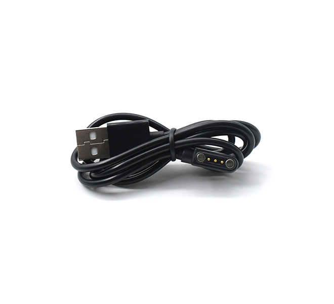
2.19 charging gun male and female pins


159-2067-7287 Mr. Wan

0769-86006029

No. 5, Zhenrong Road, Wusha, Chang'an Town, Dongguan City
 Whatapp
CopyRight © 2024 Dongguan Yongtan New Energy Co., Ltd. All Rights Reserved


 CN
CN
 Home >