


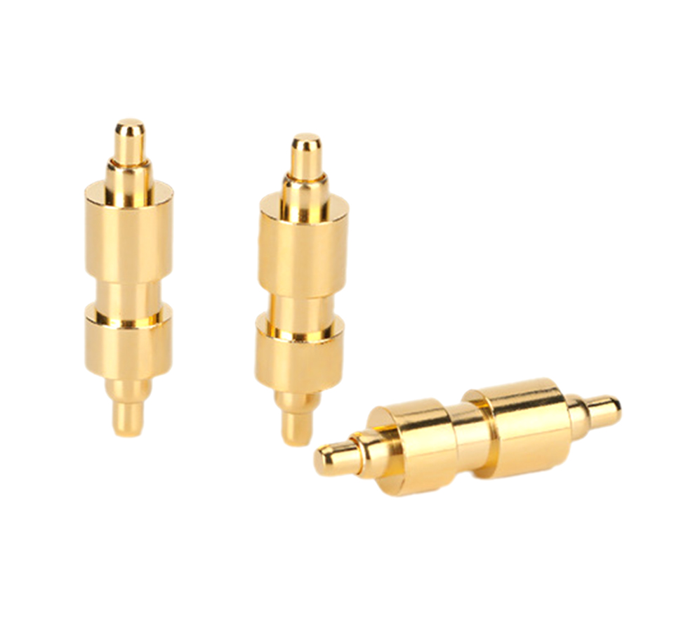
Pogopin probe arrays are highly specialized configurations that consist of multiple pogopin probes arranged in a specific pattern or layout. These arrays are designed to meet the requirements of high - density, multi - channel electrical testing and connection applications, offering enhanced functionality and efficiency compared to individual pogopin probes.
The structure of pogopin probe arrays is carefully planned to optimize the spatial arrangement of the probes while ensuring proper electrical performance. The probes are typically mounted on a common substrate, which can be a printed circuit board, a ceramic substrate, or a flexible circuit. The substrate provides mechanical support and electrical insulation for the probes and also incorporates the necessary traces and connections to route the electrical signals to and from the probes.
One of the main advantages of pogopin probe arrays is their ability to handle multiple electrical channels simultaneously. In semiconductor testing, for example, an array of pogopin probes can be used to test all the pins of a large - scale integrated circuit (LSI) or a system - on - chip (SoC) in a single test cycle. This significantly reduces the testing time and increases the productivity of the testing process. The probes in the array are precisely positioned to make contact with the corresponding pads on the device under test, ensuring accurate and reliable electrical connections for each channel.
Pogopin probe arrays also offer improved signal integrity compared to individual probes. The layout of the array can be optimized to minimize crosstalk between the channels, which is the interference between adjacent electrical signals. By carefully routing the traces on the substrate and using proper shielding techniques, the risk of crosstalk can be reduced, ensuring that each channel's signal remains pure and undistorted. Additionally, the array design can incorporate impedance - matching elements to ensure efficient signal transmission across all channels.
These arrays are widely used in various industries, including semiconductor manufacturing, electronics assembly, and research and development. In semiconductor manufacturing, pogopin probe arrays are used in wafer testing, final test, and burn - in test processes. In electronics assembly, they can be used for in - circuit testing (ICT) of printed circuit boards, where the array of probes can test all the components on the board simultaneously. As the demand for higher - density and more complex electrical testing and connection solutions continues to grow, the development of advanced pogopin probe arrays with enhanced performance and functionality will remain an important area of research and innovation in the electronics industry.
Read recommendations:


159-2067-7287 Mr. Wan

0769-86006029

No. 5, Zhenrong Road, Wusha, Chang'an Town, Dongguan City
 Whatapp
CopyRight © 2024 Dongguan Yongtan New Energy Co., Ltd. All Rights Reserved


 CN
CN
 Home >