


UFS (Universal Flash Storage) Test Pogo Pins are high-performance spring-loaded contact probes specifically designed to test UFS storage devices—next-generation storage solutions used in high-end smartphones, tablets, laptops, and automotive applications, known for their faster data transfer speeds, lower latency, and improved power efficiency compared to eMMC. These pins serve as the critical interface between test equipment and UFS chips or modules, enabling the transmission of high-speed differential signals, power, and control signals during functional, performance, and compliance testing. Given the demanding electrical requirements of UFS standards (e.g., UFS 3.1 supports data transfer rates of up to 2,900MB/s via M-PHY v5.0), UFS Test Pogo Pins are engineered to deliver exceptional signal integrity, minimal insertion loss, and robust mechanical performance, ensuring accurate and reliable testing of UFS devices.
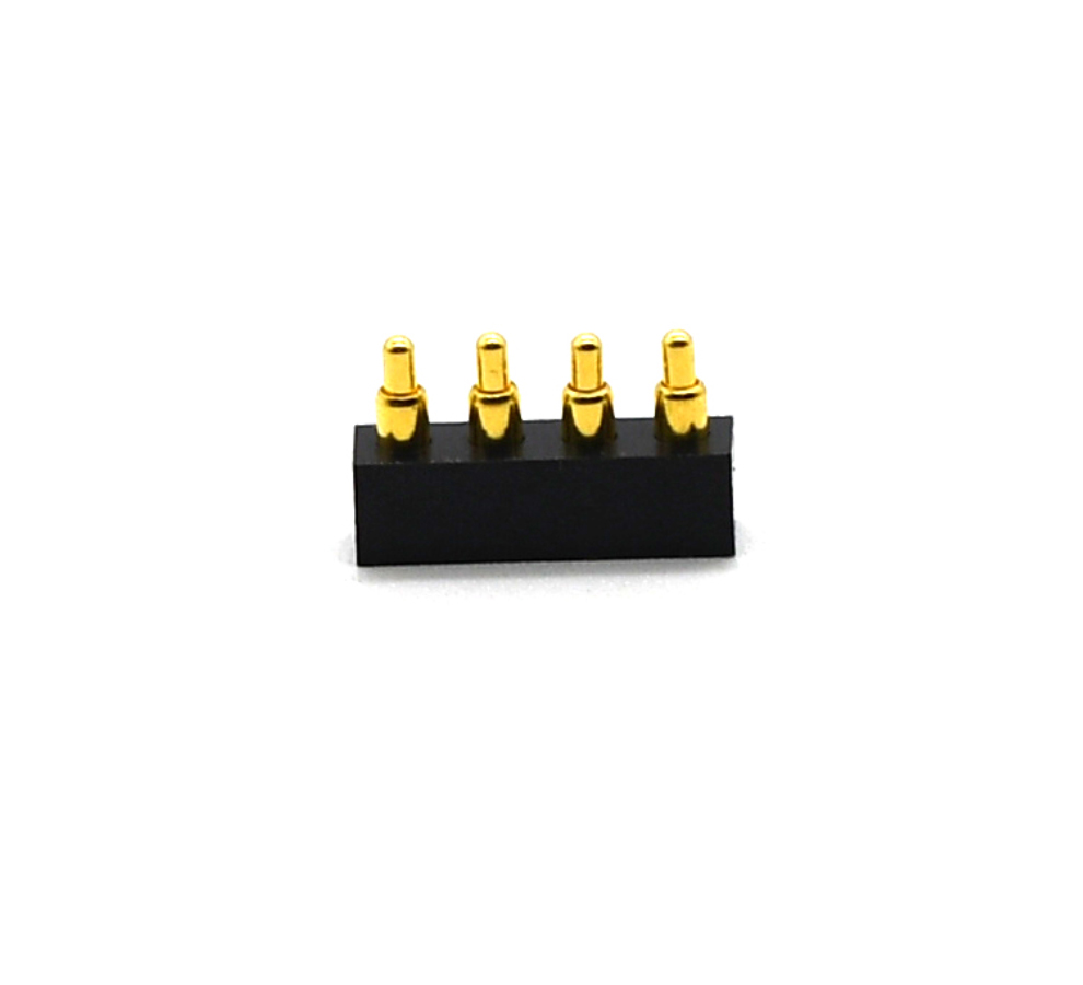
The design of UFS Test Pogo Pins is optimized for high-speed signal transmission and mechanical durability. They are typically constructed with a three-part structure: a plunger (the conductive tip), a spring (for contact force), and a barrel (the outer casing). The plunger and barrel are made from high-conductivity materials such as beryllium copper (BeCu) or phosphor bronze, which offer excellent electrical conductivity (resistivity below 1.8×10^-8 Ω·m) and mechanical strength to withstand repeated contact cycles. The plunger tip is often plated with a thick layer of gold (3-10μm) or a gold-palladium alloy to minimize contact resistance (typically below 30mΩ) and prevent oxidation, ensuring stable signal transmission even after 10,000+ test cycles. The spring, usually made of stainless steel or BeCu, is precision-engineered to apply a consistent contact force (ranging from 80g to 300g, depending on the UFS pad size and material) to avoid damaging the UFS chip’s delicate contact pads (which can be as small as 0.15mm in pitch) while maintaining a secure connection.
A key feature of UFS Test Pogo Pins is their support for differential signal pairs, which are critical for high-speed UFS communication. UFS uses M-PHY (Mobile Physical Layer) technology, which relies on differential signals (e.g., TX+/- and RX+/-) to transmit data at high speeds while minimizing electromagnetic interference (EMI) and crosstalk. UFS Test Pogo Pins are designed with matched impedance (typically 50Ω ±10%) for these differential pairs, ensuring that the signal characteristics (such as rise time, fall time, and jitter) meet the UFS specification. Additionally, the pins are spaced with precise pitch (often 0.4mm or 0.5mm) to align with the UFS chip’s contact pad layout, and their plunger tips are shaped (e.g., crown, flat, or pointed) to maximize contact area with the pad, further enhancing signal integrity.
UFS Test Pogo Pins are used in a wide range of testing scenarios to validate UFS device performance. During functional testing, they enable test equipment to send commands to the UFS chip (e.g., reading/writing data, managing power states) and verify that the chip operates correctly, including support for features like gear shifting (changing data transfer speeds dynamically) and multi-lane operation (using multiple signal lanes to increase bandwidth). In performance testing, they facilitate the measurement of data transfer speeds (sequential and random read/write), latency, and IOPS (input/output operations per second), ensuring that the UFS device meets the required performance benchmarks for high-end applications (such as 4K video recording or fast app loading). For compliance testing, the pins are used to verify that the UFS device adheres to the UFS specification (published by the JEDEC Solid State Technology Association), including electrical characteristics, signal timing, and protocol compliance.
To ensure reliability, UFS Test Pogo Pins undergo strict quality control processes. Each pin is tested for contact resistance (using a four-wire measurement method to eliminate lead resistance), spring force (using a force gauge to confirm it meets the specified range), and dimensional accuracy (using optical inspection systems to verify tip size, pitch, and alignment). Environmental testing is also performed, including temperature cycling (-40°C to 125°C), humidity testing (85% RH at 85°C), and corrosion testing (exposure to salt spray) to ensure the pins can withstand the harsh conditions of manufacturing and testing environments. Additionally, many UFS Test Pogo Pins are designed with a modular structure, allowing for easy replacement in test fixtures, which is critical for high-volume production testing where downtime must be minimized. As UFS technology continues to advance—with the development of UFS 4.0 (supporting speeds up to 4,800MB/s) and UFS Express (for PC applications)—UFS Test Pogo Pins are evolving to support even higher speeds, smaller form factors, and more stringent signal integrity requirements, making them an essential tool for UFS device manufacturing and testing.
Read recommendations:
Pogo Pin Connector Mass Production Solution
Magnetic PogoPin mass production


159-2067-7287 Mr. Wan

0769-86006029

No. 5, Zhenrong Road, Wusha, Chang'an Town, Dongguan City
 Whatapp
CopyRight © 2024 Dongguan Yongtan New Energy Co., Ltd. All Rights Reserved


 CN
CN
 Home >